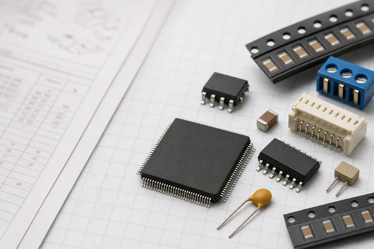
Supply volatility and cost pressure have encouraged many hardware teams to reduce single-source microcontroller exposure. GigaDevice GD32 devices are often evaluated because their peripheral concepts, development model, and Arm core options can look familiar to engineers who have worked with STM32. That familiarity is useful, but it must not be turned into a blanket drop-in claim. A successful migration starts with the exact orderable part, package drawing, pin map, memory footprint, clock tree, peripherals, electrical limits, errata, and firmware behavior. The comparison below uses STM32F405RGT6, GD32F303CCT6, and GD32F103VGT6 to show why feature overlap and pin-to-pin compatibility are different questions.
The named GD32F303CCT6 and GD32F103VGT6 devices are not pin-to-pin replacements for STM32F405RGT6: the examples use LQFP48, LQFP100, and LQFP64 packages respectively. Any migration claim must begin with an exact package and pin-map comparison.
Establish the baseline device
STMicroelectronics specifies the STM32F405RGT6 as an Arm Cortex-M4 MCU with floating-point capability, a maximum CPU frequency of 168 MHz, 1 MB of Flash, and 192 KB plus 4 KB of SRAM in a 64-pin LQFP package. The family includes a broad peripheral set: multiple ADCs, timers, DMA controllers, serial interfaces, USB OTG, and other functions whose availability depends on the package and exact device. Existing firmware may also depend on the STM32F4 clock tree, interrupt numbering, DMA stream/channel assignments, boot mode, option bytes, debug behavior, and ST HAL or LL software.
| Device | Core / maximum clock | Flash / SRAM | Package in this example | Immediate conclusion |
|---|---|---|---|---|
| STM32F405RGT6 | Cortex-M4 with FPU / 168 MHz | 1 MB / 192 KB + 4 KB | LQFP64 | Target design baseline. |
| GD32F303CCT6 | Cortex-M4 / up to 120 MHz | 256 KB / 48 KB | LQFP48 | Different pin count and substantially lower memory; not a pin-to-pin substitute. |
| GD32F103VGT6 | Cortex-M3 / up to 108 MHz | 1 MB / 96 KB | LQFP100 | Different core, pin count, SRAM capacity, clock and peripheral implementation; not a pin-to-pin substitute. |
GigaDevice describes GD32F303 as a Cortex-M4 enhanced family operating up to 120 MHz and positions corresponding GD32F303 packages as downward pin-compatible with corresponding GD32F103 devices. That statement is about relationships within specified GD32 families and matching packages. It is not evidence that GD32F303CCT6 can occupy an STM32F405RGT6 footprint. The suffix matters: C commonly identifies a 48-pin package in these examples, R a 64-pin package, and V a 100-pin package. Engineers must confirm the current manufacturer ordering table rather than relying on the letter alone.
Use a migration matrix, not a family-name shortcut
Begin with a spreadsheet that maps every used STM32F405RGT6 pin to its board net and function. Include supply pins, analog references, oscillator pins, reset, boot straps, SWD/JTAG, USB, CAN, communication buses, timer channels, ADC channels, and all GPIO alternate functions. Mark unused pins too; a pin considered harmless on the current design may be a power or reserved pin on a candidate. Repeat the exercise using the official package pinout of the exact candidate. If the package differs, the decision is a PCB redesign even when the application can be ported.
Next compare resource ceilings. A firmware image designed around 1 MB Flash and roughly 192 KB SRAM cannot be assumed to fit a GD32F303CCT6 with 256 KB Flash and 48 KB SRAM. Measure the linked binary, static RAM, heap, stack high-water mark, DMA buffers, graphics or protocol buffers, and field-update reserve. The GD32F103VGT6 offers more Flash in the cited configuration but still changes the core from Cortex-M4 to Cortex-M3 and provides much less SRAM than the STM32F405 baseline. Code using floating-point instructions, DSP extensions, or M4-specific libraries needs an explicit porting and performance plan.
Audit clocks and timing assumptions
Do not copy clock initialization register writes merely because names appear similar. Confirm allowed HSE frequency, internal oscillator tolerance, PLL multipliers and divisors, bus prescalers, Flash wait-state requirements, USB clock derivation, ADC clock limits, and timer clock multiplication. Start-up time and failure behavior can differ. The migration test should exercise cold start, brownout recovery, clock-source failure, watchdog reset, low-temperature and high-temperature start, and every low-power mode used by the product.
Software delay loops are a known migration trap. A loop calibrated by observation can change when core frequency, Flash access, compiler optimization, cache or prefetch behavior, and instruction execution change. Replace it with SysTick or a hardware timer before comparing devices. Then measure protocol timing, PWM edges, capture latency, interrupt jitter, and real-time deadlines on the bench. “The code runs faster” is not automatically an improvement if it violates sensor settling time, bus timing, or a safety sequence.
Port peripherals deliberately
ADC and analog behavior
Compare input range, reference requirements, sampling capacitance, source-impedance limits, sample-time options, calibration sequence, conversion trigger, DMA request behavior, accuracy tables, and errata. A compatible register name does not guarantee identical analog performance. Validate each production sensor across its input range and environmental limits, not just at room temperature with a potentiometer.
Timers, DMA, interrupts and communications
Map timer width, channel features, dead-time generation, break inputs, encoder mode, trigger routing, and DMA request sources. Compare DMA channel selection and arbitration, interrupt vectors and priorities, UART error handling, SPI modes, I2C timing, CAN filters, USB endpoints, and any CRC or random-number peripheral used by the application. If a bootloader or secure update flow exists, verify memory map, vector relocation, read protection, option bytes, unique identifiers, and rollback behavior.
Firmware libraries and toolchain
ST HAL source should not be relabeled and compiled against a GD32 target without review. Use the candidate manufacturer's current device headers, startup file, linker script, system clock code, peripheral library or CMSIS support, and errata. Isolate application logic from device-specific drivers where the existing code already has a boundary; do not create a broad abstraction layer solely for a one-time port. Record compiler version, optimization, linker map, programming algorithm, and debug probe configuration so the build can be reproduced.
Select a more credible candidate set
If retaining an LQFP64 footprint is mandatory, begin by searching exact 64-pin devices and compare their pin maps line by line. A GD32F405-family device may look closer in performance class than GD32F103 or GD32F303, but family-number similarity still does not prove footprint, peripheral, electrical, or software equivalence. If the PCB can change, GD32F303CCT6 and GD32F103VGT6 can be evaluated as architectural or cost candidates, with their package and resource differences treated as redesign inputs rather than exceptions.
Prototype before approving production
A controlled migration uses representative samples whose exact MPN and source evidence are recorded. Build a small batch, program it with the release candidate, and execute a written regression plan. Cover power-on reset, brownout, watchdog, bootloader and update, all communication interfaces, analog accuracy, maximum CPU and bus load, interrupt stress, thermal limits, EMC-sensitive modes, manufacturing test, and long-duration operation. Compare measurements with the STM32 baseline and define acceptable deltas before testing begins.
Procurement should not commit production quantity until engineering approves the exact candidate and revision. The RFQ should state sample quantity, packaging, date-code expectation, traceability evidence, and whether mixed lots are prohibited. Small-batch samples reduce commercial exposure, but they do not replace design validation. For STM32F405RGT6, GD32F303CCT6, GD32F103VGT6, or a closer GD32 candidate, the defensible conclusion comes from package data, pin mapping, memory analysis, firmware review, bench results, and documented approval—not from a generic “compatible” label.